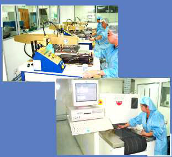
1st Stage
Screen print to circuit design interconnects and isolation pads at the conductor points onto a substrate of 96% pure Alumina or PCB board.
2nd Stage
Loading the printed solder board to placement machine for components/chip and wire process. Reflow the mounted product board follow the standard reflow profile specification.
3rd Stage
Continues to customer demand for process cutting, coating, electrical open/ short test ,rework or replace rejected board and fully visual inspection
Final Stage
Final, attachment of edge connectors or encapsulation into ceramic/metal package, whichever is appropriate.


